Nano-Electronics Area
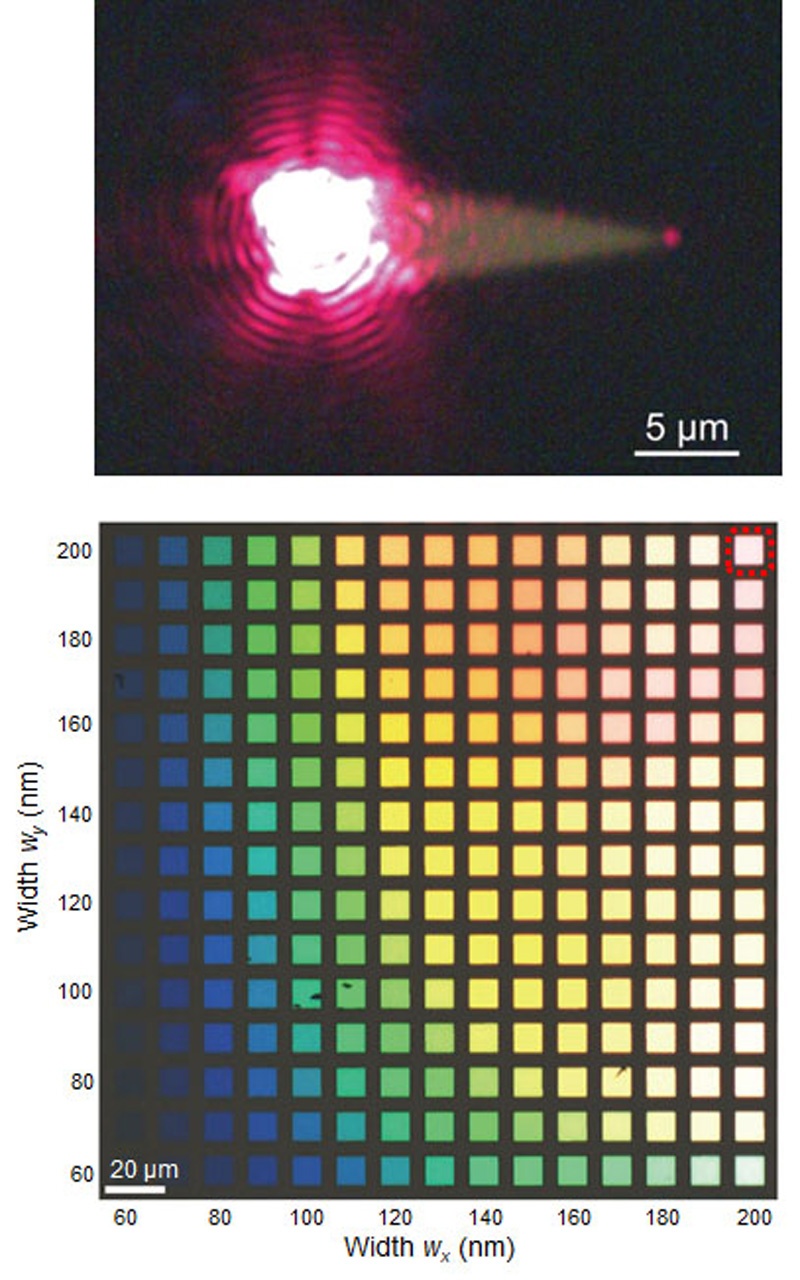
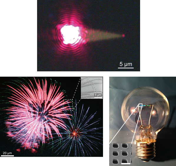
Our laboratory aims to realize innovative nanophotonic devices through basic research based on plasmonics and/or metamaterials. In metamaterials, we are conducting research on metasurfaces, which are two-dimensional metamaterials. This is an array of metal nanostructures and/or high-refractive-index dielectrics as Mie resonators arranged on a planar substrate. By controlling the scattering and absorption of meta-atoms, we have succeeded in realizing various functions such as color printing showing a diffraction limit resolution, perfect absorber and infrared emitter. At plasmonics, we are researching plasmonic waveguides and hyperbolic metamaterials. In this way, we aim to realize an ultra-fine and low power consumption photonic device that was considered impossible in principle due to the diffraction limit. In addition, by applying the metasurface-based perfect absorber to a thermal radiation filament, we have realized a prototype of a high-efficiency eco-light bulb that controls blackbody radiation.
Top