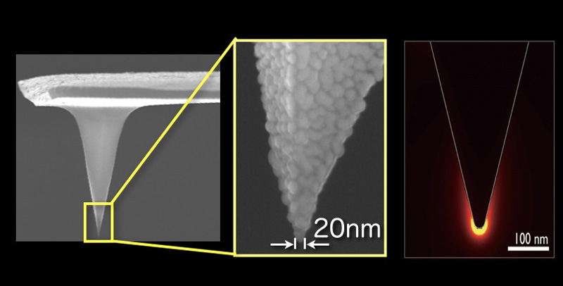
It is interesting to see nanoscale objects with light. Because the light directly interact with objects, it is possible to obtain rich information about molecular components in objects. Our group has been developing a spectroscopic technique with nanoscale spatial resolution. By combining plasmonics or near-field effect with some spectroscopic methods such as Raman scattering or photoluminescence, we can see nano-world with the visible light.
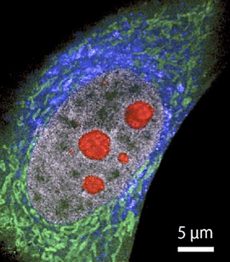
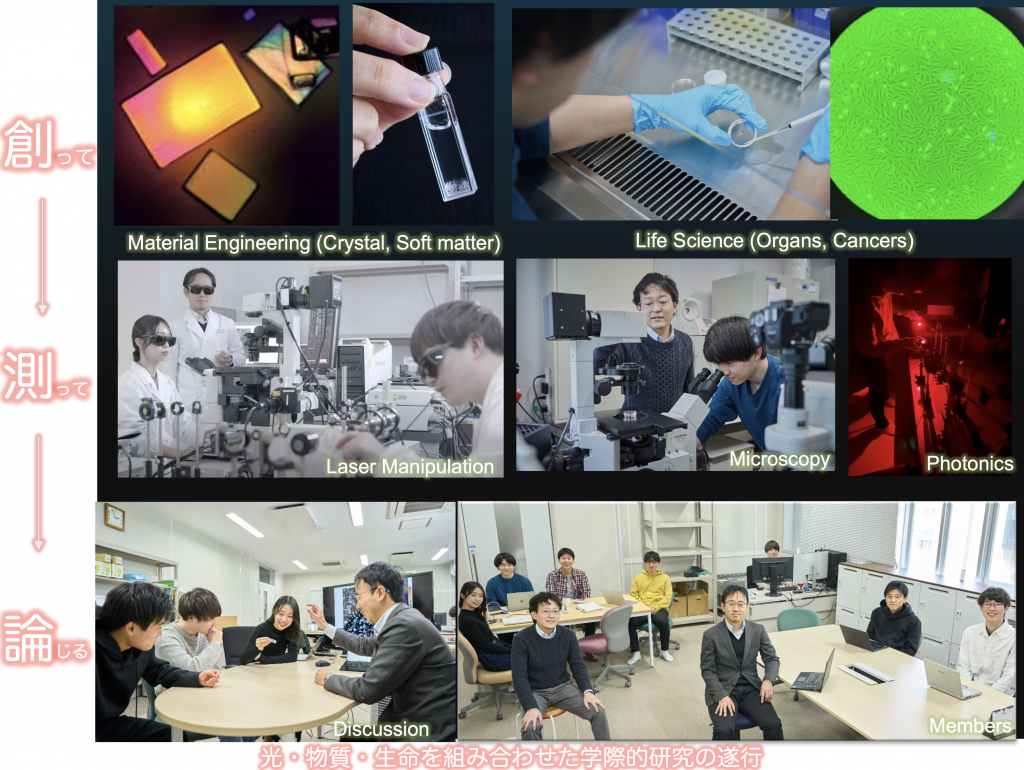
Guided by the concept of Visualizing the Invisible, our laboratory develops new optical measurement and imaging technologies based on nanophotonics, Raman spectroscopy, advanced optical microscopy, and cryogenic optical microscopy. We visualize and analyze the structure and function of cells and tissues at the molecular level, advancing understanding of life phenomena and enabling applications in disease diagnostics, drug discovery, and medicine. Through interdisciplinary research spanning physics, engineering, life sciences, and medicine, as well as international collaborations, we aim to expand the boundaries of what can be seen, measured, and understood, and to create new science and technology.
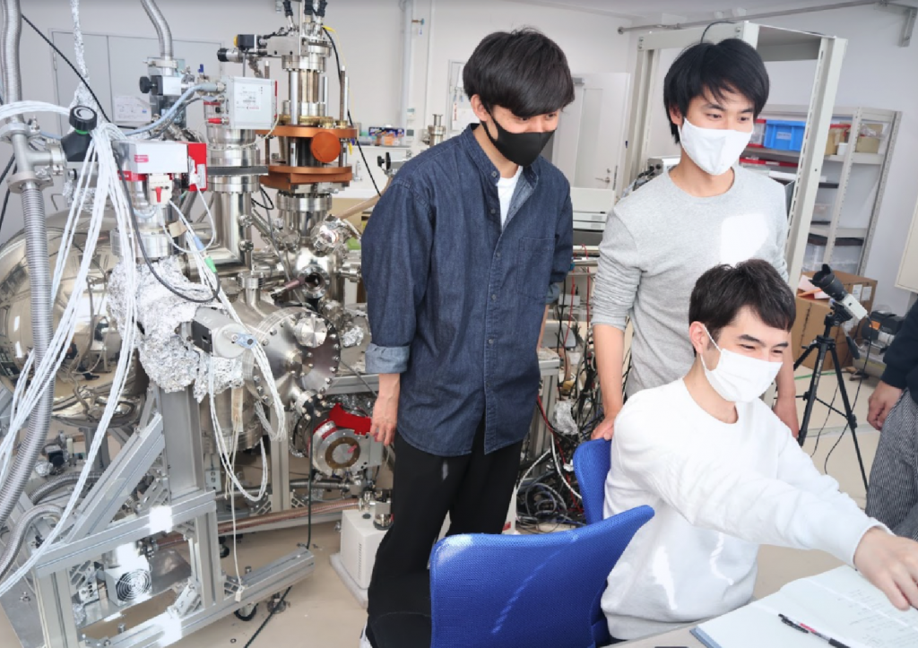
Our research interest is to investigate the unique and exotic physical phenomena of nanometer scale materials, which are formed on solid surface and do not exist in nature, and to open a new avenue toward the realization of next generation devices with high efficiency. In addition to the on-campus equipment that we have developed, we are actively conducting research at different facilities, such as synchrotron radiation facilities located all over the world.
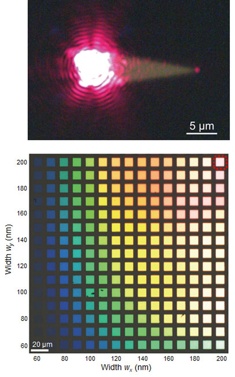
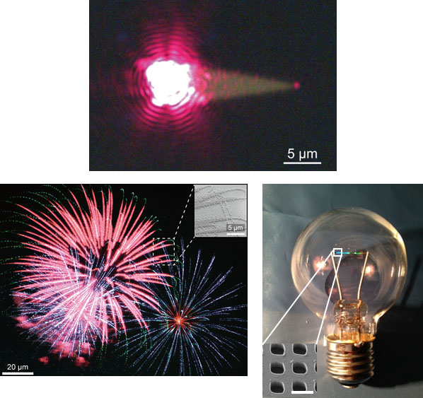
Our laboratory aims to realize innovative nanophotonic devices through basic research based on plasmonics and/or metamaterials. In metamaterials, we are conducting research on metasurfaces, which are two-dimensional metamaterials. This is an array of metal nanostructures and/or high-refractive-index dielectrics as Mie resonators arranged on a planar substrate. By controlling the scattering and absorption of meta-atoms, we have succeeded in realizing various functions such as color printing showing a diffraction limit resolution, perfect absorber and infrared emitter. At plasmonics, we are researching plasmonic waveguides and hyperbolic metamaterials. In this way, we aim to realize an ultra-fine and low power consumption photonic device that was considered impossible in principle due to the diffraction limit. In addition, by applying the metasurface-based perfect absorber to a thermal radiation filament, we have realized a prototype of a high-efficiency eco-light bulb that controls blackbody radiation.
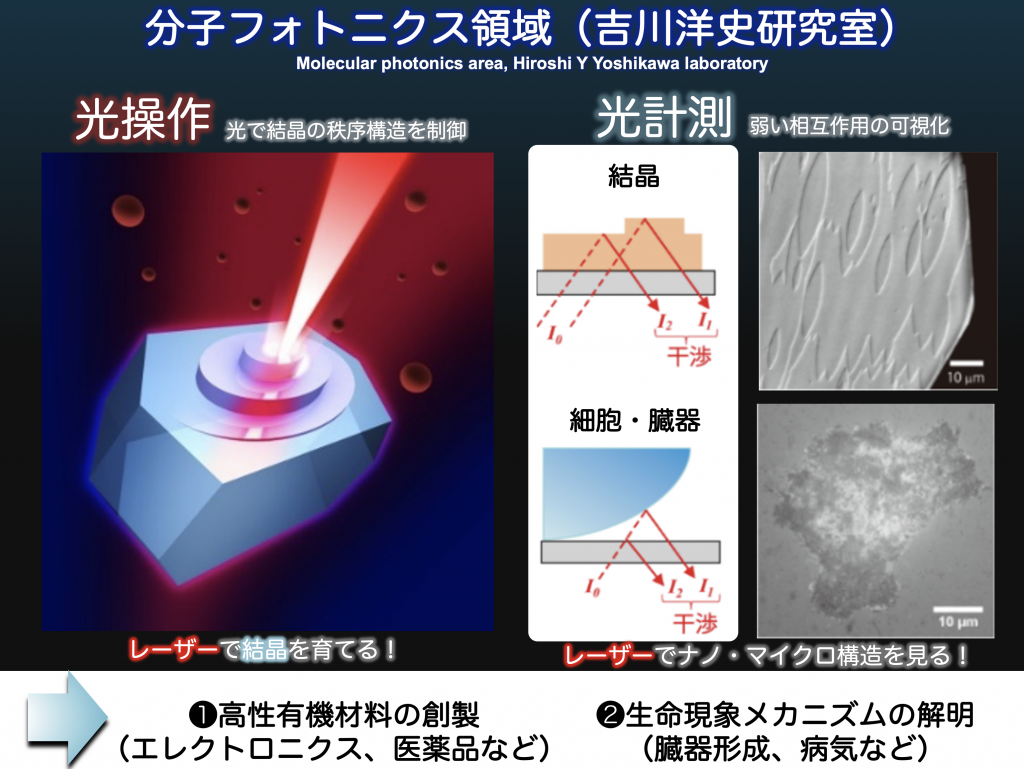
We are exploring novel materials and biological functions by using adavanced optical manipulation and measurement techniques.
1) Production of highly ordered organic and biological matters by using laser:
By utilizing physical stimuli of lasers (e.g., heat, electric field, etc) that enable us to control assembly and allighment of micro- and nano objects, we are trying to create innovative materials (electronic devices, pharmaceuticals, artificial cells, etc.) with desired structures and functions that cannot be produced by conventional methodologies alone.
2) Elucidation of unique structures and functions of soft matter:
We are investigating unique structures and functions of soft matter such as biological membranes, gels, and cellular tissue (organoids) by using non-invasive optical measurement techniques that do not disturb weak attractive and/or repulsive forces in the system.
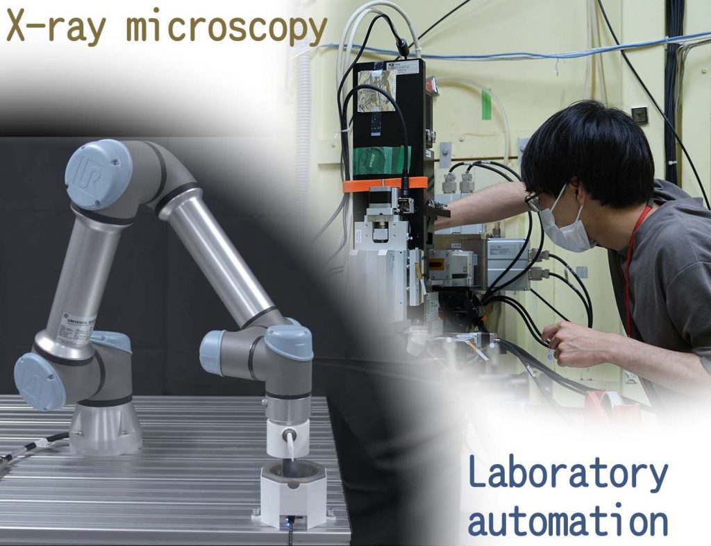
Advanced Engineering Physics Area (Ono Lab.) focuses on developing advanced advanced measurement and analysis techniques using quantum beams such as X-rays and neutrons, in combination with informatics technology. Our projects include X-ray microscopy for multi-scale characterization, machine learning-aided data analysis, laboratory automation, and AI optimization of experimental parameters.
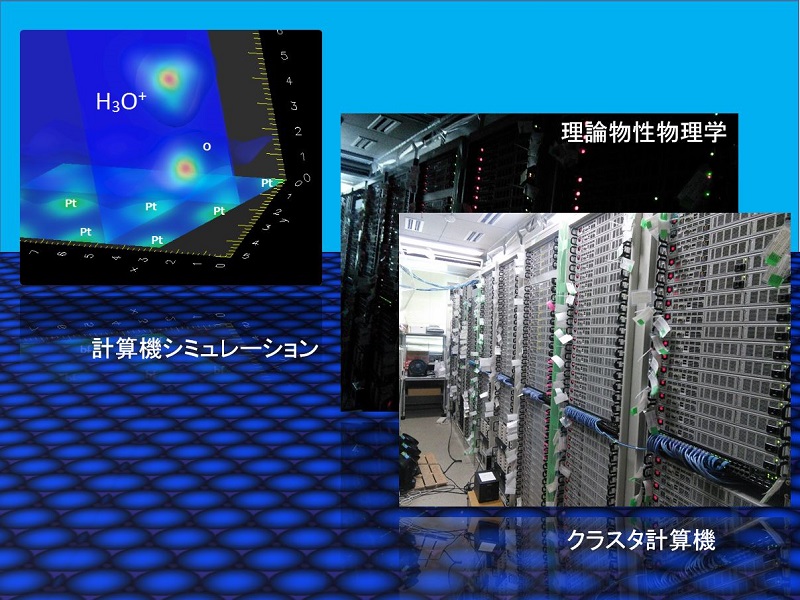
To find universality, understand the physical mechanism behind natural phenomena and the emergence of function, we conduct research and education in theoretical condensed matter physics, supported by cutting edge experimental techniques. We focus on dynamical processes and related properties at Surfaces and Interfaces of materials, size and complexity ranging from the nano-scale to biological processes. We also develop novel and practical techniques, whenever the need arises, and pro-actively make the resulting know-how available for immediate industrial implementation.
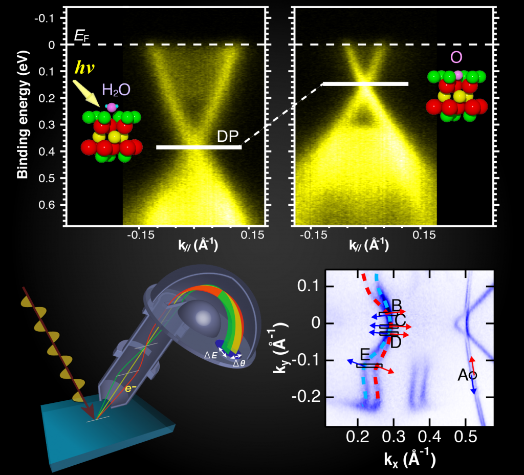
The semiconductor photocatalyst has the high resolution function for the organic matter, a self-cleaning function and photoexcited hydrophilic function, which carries the important role to various environment purification. However, the reaction mechanism has not been understood completely. We use the scanning probe microscopy (SPM) such as atomic force microscopy (AFM) and Kelvin probe force microscopy (KPFM) etc., to investigate the properties of physical and chemical, to explore and elucidate the new physical phenomena such as the photocatalyst process of the photo induced surface carrier on solid surface, liquid-solid interface. This research relates the discovery of the novelty materials with new properties of matter and can develop the catalytic design with the new function, which is different from conventional catalyst. Target one is Au NPs deposited on rutile TiO2(110) surface under gas condition at low temperature. Target two is Au NPs deposited on anatase TiO2(001) surface at low temperature. Target three is Pd nanoparticles (NPs) deposited on Al2O3/NiAl(110) surface under carbon monoxide gas (CO gas) condition.
Top